

Mapping Atomic Orbitals
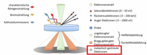

With the availability of aberration corrected electron microscopes as well as improved spectrometers, we started thinking about ways to directly map electronic states in materials in 2009. On the one hand, these electronic states are responsible for holding the matter around us together by means of electronic bonds. On the other hand, they also determine and influence many other characteristics of materials, such as optical, electric and magnetic properties. Despite their enormous importance, the direct measurement of electronic states inside of materials is quite elusive.
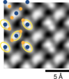
The new approach that we developed at the TU Wien uses very precise energy selection of the electron beam after it passed through the sample. This allows us to detect and measure electrons that have excited specific electronic transitions inside the sample. Just as anisotropy becomes visible in an energy-filtered diffraction pattern, this method allows to measure the direction and shape of electronic states using images with a spatial resolution below 1 Å. Our dedication to push the experimental boundaries beyond what is currently measurable is shared by our collaborators such as Ulm University, McMaster University, and the University of Antwerp.
Requests: Ass.-Prof. Dr. Stefan Löffler